Another post to file under Hacking. This one might appear to be all over the map, but the fact is I wanted to take a mikroBUS cape, BeagleBone Black, and four 4-20mA Transmitter Clickboards and build a little quad-port 4-20mA signal generator. Think of it as a hobbyists Fluke 705 Loop Calibrator.
This is without a doubt an ambitious post, and I realize its not for everyone (how many folks out there are building 4-20mA simulators with BeagleBones?). Hopefully though there are some interesting tidbits of techniques and code that anyone can lift and use in their own projects.
If you were to build everything here in this tutorial, you’re going to need:
- a BeagleBone Black
- a mikroBUS cape
- a 4-20mA T click (preferably 3 or 4 of them)
- something to read the 4-20mA signals, either the Fluke 705 or 4-20mA R click
Talking about SPI
This is not a tutorial about SPI, but suffice it to say you can come up to speed on using SPI devices with the BeagleBone Black by reading through these tutorials:
- Sparkfun’s great SPI tutorial
- Adafruit’s BeagleBone Black SPI tutorial
The upshot is that SPI, or Serial Peripheral Interface Bus, is a de facto standard for reading/writing data over a simple bus. There are hundreds of different devices that utilize a SPI interface, the 4-20mA T click that we’re interested in being one of them. Because the transmitter is a write only device, there are even fewer lines to concern ourselves with:
- 3V3 power
- Ground
- SCLK, or “clock”
- CS, aka “chip select” (also referred to as slave select)
- MOSI, aka “master-out slave-in”
SPI has often been referred to as a protocol “a first-year engineer would develop when faced with designing a bus for the first time.” It’s straightforward. Every device on the bus gets a clock line to know when to latch its inputs; everyone has the same data in and data out lines, and when the master wants to address you it lowers your chip select line (logical 0). No other device on the bus will have its chip select line low, therefore you and the master are free to send on the data lines.
Since we are going to leverage the mikroBUS cape to allow us to populate 4 4-20mA T clickboards, that means in total we’ll have 4 different SPI devices. In reality, there are 6 SPI devices here: 2 masters and 4 slaves.
Our first master is referred to on the BeagleBone Black platform as SPI0. It has one chip select brought out to the expansion header, and most examples you see online will refer to this device tree overlay. Since we’re going to be writing our own overlay, its instructive to look at this one first.
|
1 2 3 4 5 6 7 8 |
spi0_pins_s0: spi0_pins_s0 { pinctrl-single,pins = < 0x150 0x30 /* spi0_sclk, INPUT_PULLUP | MODE0 */ 0x154 0x30 /* spi0_d0, INPUT_PULLUP | MODE0 */ 0x158 0x10 /* spi0_d1, OUTPUT_PULLUP | MODE0 */ 0x15c 0x10 /* spi0_cs0, OUTPUT_PULLUP | MODE0 */ >; }; |
A lot of tutorials out there gloss over some of the details here, and quite frankly at times I don’t blame them because it can be a little mindnumbing reading through all the hex and business about INPUT_PULL | MODE0. But these values do actually map to something and MODE0 means something particular on the BeagleBone Black. What these four lines of code are declaring are the actual lines that are carrying the SPI0 signals for SCLK, chip select, and what are referred to here as D0 and D1. Why are they called D0 and D1 and not MOSI and MISO? Who knows, but you can tell which is which because:
- D0 is labeled as an INPUT, therefore data is coming from the slave into the master, so it is the MISO line
- D1 is labeled as an OUTPUT, therefore data is going out from the master into the slave, so it is the MOSI line
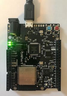
So where do these lines come out on the BBB Expansion header? A quick way to determine is to take a look at https://github.com/jadonk/bonescript/blob/master/src/bone.js and simply search for 0x150. You’ll find that its P9_22. For 0x154 you can quickly find out that it is P9_21. You can also look at this image illustrating the SPI pins:
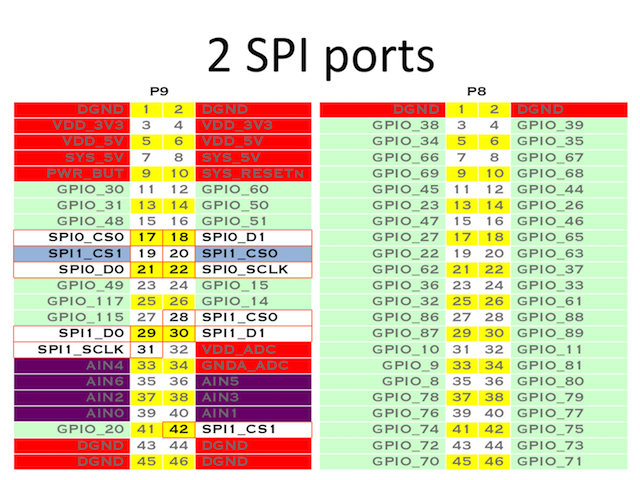
Take a look again at the overlay above and how the 4 pins iterated line up with what the image above shows. It’s instructive when you look at SPI1, which has another chipselect line, cs1, brought out to the header.
mikroBUS Cape
The mikroBUS Cape opens up the possibility of having 4 SPI slaves, but one must be mindful that that isn’t the physical default. If you look carefully at the manual schematic, you’ll see that “host 3” by default does not have the SCLK and MISO lines connected, but rather are jumpered as RX/TX lines (presumably for working with UART devices). If you flip the cape over on the back you can see this jumpering:
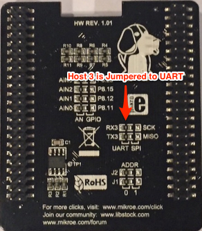
You can also see that Host 3 is jumpered to UART by default in the cape manual:
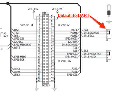
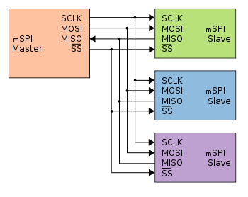
For the remainder of this tutorial, until I get someone more savvy with SMD components than I am, we’ll focus on Host 1, 2, and 4, which fortuitously map directly to the SPI1 device on the BeagleBone. It also maps nicely to this diagram from the SPI Wikipedia entry:
To get our BeagleBone ready, we’re going to have to write a Device Tree Overlay just for us. We’ll call it BBB-SPICAPE to reiterate the fact that we’re looking to have all SPI devices on our cape. To be clear, this overlay is not for the generic use of the mikroBUS cape! If you are plugging in clickboards that make use of the UART lines, it will look completely different!
Here’s what the file looks like in all its arcane glory:
/dts-v1/;
/plugin/;
/ {
compatible = "ti,beaglebone", "ti,beaglebone-black";
/* identification */
part-number = "BB-SPICAPE-01";
version = "00A0";
/* state the resources this cape uses */
exclusive-use =
/* the pin header uses */
"P9.17", /* spi0_cs0 */
"P9.18", /* spi0_d1 */
"P9.21", /* spi0_d0 */
"P9.22", /* spi0_sclk */
"P9.28", /* spi1_cs0 */
"P9.29", /* spi1_d0 */
"P9.30", /* spi1_d1 */
"P9.31", /* spi1_sclk */
"P9.42", /* spi1_cs1 */
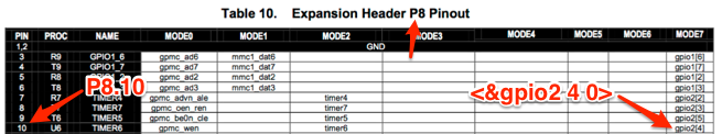
"P8.10", /* spi1_cs2, but not really */
/* the hardware ip uses */
"spi0",
"spi1",
"gpio2_4";
fragment@0 {
target = <&am33xx_pinmux>;
__overlay__ {
/* avoid stupid warning */
#address-cells = <1>;
#size-cells = <1>;
my_gpio_pins: pinmux_my_gpio_pins {
pinctrl-single,pins = <
/* the gpio pin(s) */
0x098 0x17 /* P8 10 gpio2_4.spi1_cs2 OUTPUT_PULLUP | MODE7 */
>;
};
bb_spi0_pins: pinmux_bb_spi0_pins {
pinctrl-single,pins = <
0x150 0x30 /* spi0_sclk.spi0_sclk, INPUT_PULLUP | MODE0 */
0x154 0x30 /* spi0_d0.spi0_d0, INPUT_PULLUP | MODE0 */
0x158 0x10 /* spi0_d1.spi0_d1, OUTPUT_PULLUP | MODE0 */
0x15c 0x10 /* spi0_cs0.spi0_cs0, OUTPUT_PULLUP | MODE0 */
>;
};
bb_spi1_pins: pinmux_bb_spi1_pins {
pinctrl-single,pins = <
0x190 0x33 /* mcasp0_aclkx.spi1_sclk, INPUT_PULLUP | MODE3 */
0x194 0x33 /* mcasp0_fsx.spi1_d0, INPUT_PULLUP | MODE3 */
0x198 0x13 /* mcasp0_axr0.spi1_d1, OUTPUT_PULLUP | MODE3 */
0x19c 0x13 /* mcasp0_ahclkr.spi1_cs0, OUTPUT_PULLUP | MODE3 */
0x164 0x12 /* eCAP0_in_PWM0_out.spi1_cs1 OUTPUT_PULLUP | MODE2 */
>;
};
};
};
fragment@1 {
target = <&ocp>;
__overlay__ {
spi1_cs2 {
compatible = "gpio-of-helper";
status = "okay";
pinctrl-names = "default";
pinctrl-0 = <>;
P8_10 {
gpio-name = "spi1_cs2";
gpio = <&gpio2 4 0>;
output;
init-high;
};
};
};
};
fragment@2 {
target = <&spi0>; /* spi0 is numbered correctly */
__overlay__ {
status = "okay";
pinctrl-names = "default";
pinctrl-0 = <&bb_spi0_pins>;
#address-cells = <1>;
#size-cells = <0>;
spi0@0{
#address-cells = <1>;
#size-cells = <0>;
compatible = "spidev";
reg = <0>;
spi-max-frequency = <16000000>;
spi-cpol;
spi-cpha;
};
};
};
fragment@3 {
target-path = "/ocp/interrupt-controller@48200000";
__overlay__ {
#gpio-cells = <2>;
};
};
fragment@4 {
target = <&spi1>; /* spi1 is numbered correctly */
__overlay__ {
status = "okay";
pinctrl-names = "default";
pinctrl-0 = <&bb_spi1_pins>;
#address-cells = <1>;
#size-cells = <0>;
cs-gpios = <0>, <1>, <&gpio2 4 0>;
spi1@0 {
#address-cells = <1>;
#size-cells = <0>;
compatible = "spidev";
reg = <0>;
spi-max-frequency = <16000000>;
spi-cpol;
spi-cpha;
};
spi1@1 {
#address-cells = <1>;
#size-cells = <0>;
compatible = "spidev";
reg = <1>;
spi-max-frequency = <16000000>;
spi-cpol;
spi-cpha;
};
spi1@2 {
#address-cells = <1>;
#size-cells = <0>;
compatible = "spidev";
reg = <2>;
spi-max-frequency = <16000000>;
spi-cpol;
spi-cpha;
};
};
};
};
There are few things to note here:
I could not get chip select 2 working “automatically” as a part of the Linux SPI driver. Supposedly I should have been able to specify cs-gpios and include the tag <&gpio2 4 0> and that would magically associate the underlying GPIO pin with the chipselect and it would “just work.” Unfortunately it didn’t, but there’s a workaround which I’ll outline in a bit. After quite a bit of searching online I came across this thread where someone writes:
Incidentally, the spi-omap2-mcspi.c driver does not support a GPIO as a chip select.
Now, whether or not that’s true, I’m not one to say. I read through the source code and considered putting in some additional debug statements to trace things down but in the end moved on.
If you know how to get to use one of the GPIO pins configured as a SPI chip select on a BeagleBone, drop me a line!
To compile and prepare our device tree overlay for installation:
dtc -O dtb -o BB-SPICAPE-01-00A0.dtbo -b 0 -@ BB-SPICAPE-01-00A0.dts
cp BB-SPICAPE-01-00A0.dtbo /lib/firmware
Disabling HDMI
If you Google BeagleBone Black SPI1 you will undoubtedly run across the admonishment that you must disable HDMI to use SPI1! They aren’t joking, and the reason why is that the HDMI chip on the Black uses pins that SPI1 uses too. So you have to pick. You get HDMI, or you get SPI1. So in your /boot/uEnv.txt add this line:
|
1 |
cape_disable=bone_capemgr.disable_partno=BB-BONELT-HDMI,BB-BONELT-HDMIN |
You might also have to track down a line in /boot/uEnv.txt and remove cape_universal=enable; that loads a “universal cape” overlay that conflicts with our use.
You might also have to add:
|
1 |
dtb=am335x-boneblack-emmc-overlay.dtb |
in /boot/uEnv.txt on 4.x kernels.
Loading our DTBO
After you’ve copied the BB-SPICAPE-01-00A0.dtbo file to /lib/firmware, and you’ve disabled the HDMI overlays in /boot/uEnv.txt, reboot your BeagleBone Black. Review the contents of the Cape Manager slots file to make sure there are no overlays installed.
root@beaglebone:~# cat /sys/devices/platform/bone_capemgr/slots
 0: PF----  -1
 1: PF----  -1
 2: PF----  -1
 3: PF----  -1
Now let’s load our overlay!
root@beaglebone:~# echo BB-SPICAPE-01 > /sys/devices/platform/bone_capemgr/slots
If the load was successful you’ll see the following at the end of dmesg.
[   30.422918] bone_capemgr bone_capemgr: part_number 'BB-SPICAPE-01', version 'N/A'
[   30.422960] bone_capemgr bone_capemgr: slot #4: override
[   30.422978] bone_capemgr bone_capemgr: Using override eeprom data at slot 4
[   30.422996] bone_capemgr bone_capemgr: slot #4: 'Override Board Name,00A0,Override Manuf,BB-SPICAPE-01'
[   30.448839] gpio-of-helper ocp:spi1_cs2: Allocated GPIO id=0
[   30.448868] gpio-of-helper ocp:spi1_cs2: ready
[   30.451031] bone_capemgr bone_capemgr: slot #4: dtbo 'BB-SPICAPE-01-00A0.dtbo' loaded; overlay id #0
[   30.510242] spi spi2.2: not using DMA for McSPI
You should also see that 4 SPI devices were created in /dev and that gpio68 is present in /sys/class/gpio:
root@beaglebone:~# ls -l /dev/spi*
crw-rw---- 1 root spi 153, 0 Nov 28 17:10 /dev/spidev1.0
crw-rw---- 1 root spi 153, 3 Nov 28 17:10 /dev/spidev2.0
crw-rw---- 1 root spi 153, 2 Nov 28 17:10 /dev/spidev2.1
crw-rw---- 1 root spi 153, 1 Nov 28 17:10 /dev/spidev2.2
root@beaglebone:~# ls -l /sys/class/gpio/gpio68
lrwxrwxrwx 1 root root 0 Nov 28 17:18 /sys/class/gpio/gpio68 -> ../../devices/platform/ocp/481ac000.gpio/gpio/gpio68
Protocols, Protocols
Whereas SPI provides the physical means of communicating with a SPI device, one must still learn the specifics of how to write, read, and interpret data from a given device. For example, a 256 Kbit Serial SRAM SPI chip will likely have a set of commands to write to the device (and into what memory location), and certain commands to read from the device. Likewise, our 4-20mA devices have a specific protocol for communicating with them.
For some reason MikroElektronika buries its protocols in example code, so when you get a new little clickboard to play with you have to go digging through source code and reverse engineering the protocol out of it.
For the 4-20mA transmitter the code says that the device “performs linear conversion of input number from range 800 – 4095 into current in range 4mA – 20mA”. So we know if we write 800 to the device it will output 4mA. Writing 4095 will cause it to output 20mA. That part is easy, the tricky part is to know how to tell the device to write.
SPI is byte-oriented protocol, i.e., you send a byte at a time. Reviewing the source code example for the 4-20mA T click, we see that its write protocol is to send two bytes formatted as follows:
  1 1 1 1 1 1
  5 4 3 2 1 0 9 8   7 6 5 4 3 2 1 0
+-----------------------------------+
| 0 0 1 1 x x x x | x x x x x x x x |
+-----------------------------------+
that is, where bits 12-15 are 0x3 (think of it as the WRITE_COMMAND), and bits 11-0 is 800 through 4095.
I’m going to be using NodeJS for this application, so, I can accomplish this through:
|
1 2 3 4 |
var val = mikro |= 0x3000 var mbuf = new Buffer(2) buf.writeUInt16BE(val,0) spi12.transfer(mbuf, new Buffer(mbuf.length)) |
Don’t copy/paste the above code anywhere, it’s just an illustration that we want to write an uint16 out to the SPI device. You might be asking yourself (because I certainly did), “What is that new Buffer(mbuf.length) business all about?” That is a result of SPI being a “clock-in, clock-out” protocol. From the SPI Wikipedia entry:
During each SPI clock cycle, a full duplex data transmission occurs. The master sends a bit on the MOSI line and the slave reads it, while the slave sends a bit on the MISO line and the master reads it. This sequence is maintained even when only one-directional data transfer is intended.
That is, sending a byte down the MOSI (master-out slave-in) line results in a byte coming in on the MISO (master-in slave-out) line.
That’s the 4-20mA T click, let’s look at the R click. Believe it or not (and when you see the example code, you will), to read the 4-20mA R click you write 2 bytes, and then read the received 2 bytes as follows:
  1 1 1 1 1 1
  5 4 3 2 1 0 9 8   7 6 5 4 3 2 1 0
+-----------------------------------+
| _ _ _ x x x x x | x x x x x x x _ | // ADC = bits[12:1]
+-----------------------------------+
The underscores just highlight that these are “don’t care” bits.
No kidding, here is the example source code from Mikro:
|
1 2 3 |
adc_h = SPI1_Read(0x12) & 0x1F; // Get upper 4 bits of ADC value adc_l = SPI1_Read(0x12); // Get upper 8 bits of ADC value adc_s[i] = ( ( adc_h << 8 ) | adc_l) >> 1; // Add ADC value to checkup array |
The first byte is read and masked with 0x1F, thus getting the lower 5 bits, then the second byte is taken. The 5 bits from the first byte then get shifted to the upper 8 bits of a uint16 and bitwise-ored with the second byte. This is then shifted one bit to the right (notice the _ in bit 0 above? That’s what gets shoved off the edge with our shift-right).
A much simpler version in NodeJS:
|
1 2 3 |
var outbuf = new Buffer(2) reader0.transfer(outbuf, outbuf) var adc = (outbuf.readUInt16BE() & 0x1fff) >> 1 |
Controlling with NodeJS
The ultimate goal of this project is to develop a NodeJS Express application which will expose a web interface for manipulating the 4-20mA transmitters. There is a handy SPI module on NPM that we’ll use, so let’s get started installing NodeJS and our SPI module:
curl -sL https://deb.nodesource.com/setup_4.x | bash -
apt-get install -y nodejs
npm install spi
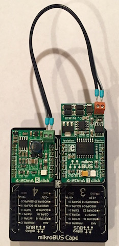
The mikroBUS cape identifies each clickboard slot with a number, so we’ll use that number in our code. Slot (or “host”) 1 has a 4-20mA receiver in it, and slot 2 has a 4-20mA transmitter. The two have been connected creating a functioning 4-20mA loop.
|
1 2 3 4 5 6 7 8 9 10 11 12 13 |
var SPI = require('spi') var milliamps = process.argv[2] var receiver1 = new SPI.Spi('/dev/spidev2.0', { 'mode':SPI.MODE['MODE_0'], 'chipSelect':SPI.CS['low'] }, function(s){s.open()}) var transmitter2 = new SPI.Spi('/dev/spidev2.1', { 'mode':SPI.MODE['MODE_0'], 'chipSelect':SPI.CS['low'] }, function(s){s.open()}) |
It’s important to recognize that the above spidev devices were created when we added our device tree overlay, and that the notation is /dev/spidevMASTER.CHIPSELECT_REG. In this case MASTER is SPI1, which is in the filesystem as spidev2. The cs0 line for SPI1 is to Slot 1, and the cs1 line for SPI1 is to Slot 2.
Note: Working with SPI on the BeagleBone Black can be confusing with the “off-by-one” business. BeagleBone documentation refers to the two SPI devices as SPI0 and SPI1, but they are presented by the Linux SPI module as /dev/spi1.X and /dev/spi2.X. What is even more confusing is if you unload and reload the overlay, Linux will create /dev/spi3.X and /dev/spi4.X!
Continuing, we need two functions here to convert to and from the 12-bit ADC range of 800-4095 to 4-20mA:
|
1 2 3 4 5 6 7 8 9 10 11 |
function milliampsToMikro(milliamps) { var mikro = (205.9375*milliamps) - 23.75 if (mikro < 800) mikro = 800 if (mikro > 4095) mikro = 4095 return mikro } function mikroToMilliamps(mikro) { var milliamps = (mikro*0.004855842) + 0.115326252 return milliamps } |
If you deal with 4-20mA much you’ll get used to doing these linear equations. In the first example we want to map 4-20mA to 800-4095. Doing the math we get the first equation:

The second equation reverses the process.
Now, let’s use our knowledge of the T click and R click to write out what we want to transmit and then reread it on the receiver.
|
1 2 3 4 5 6 7 8 9 10 11 12 13 14 15 16 |
var mikro = milliampsToMikro(milliamps) console.log("Milliamps: " + milliamps) console.log("Output to Transmitter: " + mikro) var val = mikro |= 0x3000 var mbuf = new Buffer(2) mbuf.writeUInt16BE(val,0) transmitter2.transfer(mbuf, mbuf) var outbuf = new Buffer(2) receiver1.transfer(outbuf, outbuf) var adc = (outbuf.readUInt16BE() & 0x1fff) >> 1 console.log("Input from Receiver: " + adc) console.log("Millamps: " + mikroToMilliamps(adc)) |
Our first step is to convert the command-line argument (which we expect to be milliamps) to the 800-4096 range. We then perform the required operations to write to the device via SPI (bit-or with 0x3000). After transmitting we then read from our receiver to see what it is detecting as the loop current. Again, half of the battle with SPI is knowing the exact format of how to write and read values to the device in question. Running our app we get:
# node outputMilliamps.js 12
Milliamps:              12
Output to Transmitter:  2447.5
Input from Receiver:    2467
Millamps:               12.094688466
Of course, this is an opportunity to determine what policy you’re going to have on precision and how many times you want to sample the receiver. The mikro code for the R click samples a dozen or so times and tosses out the min and max value of what is read. We won’t worry about that for now but will move on to using our 3rd SPI device (SPI1 chipselect 2), which is a little trickier.
Manual Chip Select
If you recall from above, I said that I couldn’t get the chipselect line for Host 4 (on the cape) working. Well, that’s partially true. I couldn’t get it to automatically work, as in, when using the code above like receiver1.transfer(outbuf,outbuf), you’ll notice that’s it. The Linux SPI driver takes care of lowering the chip select line to talk to the device. This works for both chip select 0 and 1, but I could not getting it working for 2. So we’ll just do it manually like this:
|
1 2 3 4 |
fs.writeFile('/sys/class/gpio/gpio68/value', 0, function() { transmitter4.transfer(mbuf, mbuf) fs.writeFile('/sys/class/gpio/gpio68/value', 1, readReceiver) }) |
Here we simply drive gpio68 low, engage our SPI device, and then raise the pin. We’ve done by hand what the Linux SPI driver handled for us in the previous example.
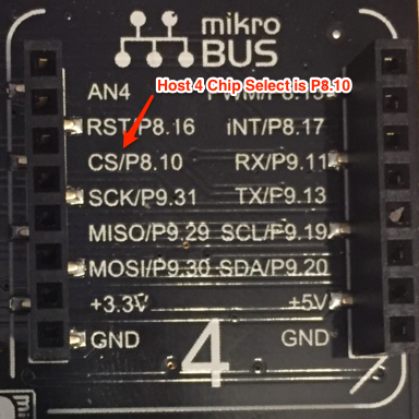
Why gpio68? That’s the GPIO line that maps to P8.10 on the BeagleBone header, which in turn is delivered to our mikroBUS cape. You can see that by reading the identifiers on the cape itself:
This is also why our device tree overlay specifies the GPIO pin like this:
|
1 2 3 4 5 6 |
P8_10 { gpio-name = "spi1_cs2"; gpio = <&gpio2 4 0>; output; init-high; }; |
If you look at the BeagleBone System Reference Manual, you’ll see too that all of these references like <&gpio 2 4 0> actually do map back to something:
We want the pin to be specified as an output, and to initialize it high, or logical 1. If we didn’t do this the pin could float, or worse, be driven low, which would in effect mean it was always in a “selected mode.” The Linux SPI driver would have no knowledge of this and multiple SPI devices would be talking on the bus. Which, of course, is a no-no.
Our readReceiver function looks like this:
|
1 2 3 4 5 6 7 |
function readReceiver() { var outbuf = new Buffer(2) receiver1.transfer(outbuf, outbuf) var adc = (outbuf.readUInt16BE() & 0x1fff) >> 1 console.log("Input from Receiver: " + adc) console.log("Millamps: " + mikroToMilliamps(adc)) } |
Note that we wait for the result of raising the chip select line before reading the receiver. Remember, we’re working with Node here, so we have to be explicit about when to read the result of writing to our SPI transmitter. Otherwise we could have charged ahead and read the receiver before the transmitter had been written to, thus resulting in stale data.
Measuring with a Fluke 705 Loop Calibrator
The 4-20mA transmitter clickboard from MikroElectronika does not supply the power for the current loop. The 4-20mA receiver, when paired with the transmitter, can supply this power (~15V), but if you are using the transmitter in other applications you’ll need to provide it yourself. For example, if you want to test the output of your transmitter with a Fluke 705 you’ll need to have a circuit like this:

Note: This is best done with a DC power supply. A fresh 9V battery will work, but you’d be surprised how quickly you can drain a battery pulling 20mA!
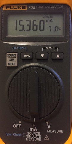
Once connected, turn the Fluke 705 to the mA Source/Simulate/Measure setting, and then press the Source/Sim/Measure button until the device reads MEASURE on the display. Use the NodeJS code to tell the transmitter to set the loop to, say, 15mA. The result:
Getting the Code
This tutorial is by no means complete, and we still don’t have a working Express application. That will be added at a later date! In the meantime, you can download the device tree overlay and working NodeJS applications for reading/writing to the 4-20mA clickboards on GitHub.
Once you have the code, run make node to download and install NodeJS 4.x. If you don’t need to install NodeJS you can skip directly to make npm to install the SPI npm module.
To compile the overlay, run make (or make dtbo). This will compile and copy the overlay to /lib/firmware. Don’t forget to edit /boot/uEnv.txt and disable HDMI!. Reboot after making the appropriate changes to /boot/uEnv.txt.
Note: I’ve had issues at times loading the device tree overlay. For some reason the kernel will occasionally lock up in systemd-udevand it will be lights out until the board is reset. I haven’t tracked down why this occurring yet!

How to disable hdmi from am335x-boneblack.dts.
There are too many problems with uEnv.txt configuration with different kernel versions and OS distros. I just want to get rid of the hdmi for good.
Hope you can shed some light on this issue.
Many thanks.